☰
Wave Optics
(a) Describe briefly, with the help of a diagram, the role of the two important processes involved in the formation of a p-n junction.
(b) Name the device which is used as a voltage-regulator. Draw the necessary circuit diagram and explain its working.
OR
(a) Explain briefly the principle on which a transistor-amplifier works as an oscillator. Draw the necessary circuit diagram and explain its working.
(b) Identify the equivalent gate for the following circuit and write its truth table.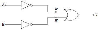
a) Important process occurring during the formation of p-n junction are:
1) Diffusion: When p-n junction is formed due to concentration gradient, the holes diffuse from p-side to n-side and electrons diffuse from n-side to p-side. This motion of charge carriers gives rise to diffusion current across the junction.
2) Drift: Drift of charge carriers occurs due to the applied electric field. As a result of the potential barrier, an electric field from n-region to p-region is developed across the junction. This electric field causes motion of electrons on p-side of the junction to n-side of the junction. Holes are moved from n-side to p-side. Thus, a drift current starts which is opposite to the direction of diffusion current.
b) Zener diode is used as voltage regulator. 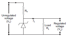
There is a voltage drop across Rs whenever there is decrease or increase in the input voltage. Change in voltage across Rs does not affect the voltage across Zener diode.
OR
a) The below fig. is that of a transistor amplifier.
The transistor amplifier works on the principle of mutual induction.
The above circuit contains tuned circuit made of variable capacitor C and an inductor L in the collector circuit and hence is named as tuned collector oscillator. The feedback coil L¢ connected to base circuit is mutually coupled with coil L.
The biasing is provided by emitter resistance RE and potential divider arrangement consisting of resistances R1 and R2. The capacitor C1 connected in the base circuit provides low reactance path to the oscillations and the capacitor CE is the emitter by-pass capacitor so that the resistor RE has no effect on the ac operation of the circuit.
Closing switch S will switch on the collector supply voltage. So, collector current starts increasing and capacitor C is charged. When the capacitor attains maximum charge, it discharges through coil L , setting up oscillations of natural frequency which is given by, 
These oscillations induce a small voltage in coil L’ by mutual induction. This induced voltage is the feedback voltage; its frequency is same as that of resonant LC circuit but its magnitude depends on the number of turns in L’ and coupling between L and L’ . The feedback voltage is applied between the base and emitter and appears in the amplified form in the collector circuit. A part of this amplifier energy is used to meet losses taking place in oscillatory circuit to maintain oscillations in tank circuit and the balance is radiated out in the form of electromagnetic waves.
b) The Boolean expression for the output is given by, 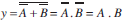
This is the expression for AND gate.
Symbol for AND gate is given by, 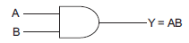
Truth table is given by, 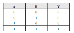


Sponsor Area
Sponsor Area
Sponsor Area