☰
Semiconductor Electronics: Materials, Devices and Simple Circuits
The reason of current flow in p-n junction in forward bias is
drifting of charge carriers
drifting of minority charge carriers
diffussion of charge carriers
All of the above
C.
diffussion of charge carriers
In forward biased condition, the width of the depletion region is very narrow. Hence, the free electrons and holes easily overcome the weak opposite electric field from the depletion region and cross the depletion region. Therefore, the electric current flows in the forward biased condition.
Due to diffusion of charge carriers current flows throw in p-n junction.


Sponsor Area
The logic circuit shown below has the input waveforms ‘A’ and ‘B’ as shown. Pick out the correct output waveform.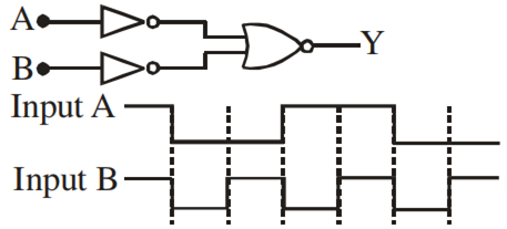
output is
A working transistor with its three legs marked P, Q and R are tested using a multimeter. No conduction is found between P and Q. By connecting the common (negative) terminal of the multimeter to R and the other (positive) terminal of P or Q, some resistance is seen on the multimeter. Which of the following is true for the transistor?
In the circuit below, A and B represent two inputs and C represents the output. The circuit represents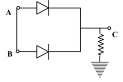
If in a p-n junction diode, a square input signal of 10V is applied as shown Then the output signal across RL will be 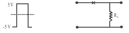
Carbon, silicon and germanium have four valence electrons each. At room temperature which one of the following statements is most appropriate?
A thermocouple is made from two metals, Antimony and Bismuth. If one junction of the couple is kept hot and the other is kept cold then, an electric current will
A solid which is transparent to visible light and whose conductivity increases with temperature is formed by
In a common base mode of a transistor, t collector current is 5.488 mA for an emit current of 5.60 mA. The value of the base current amplification factor (β) will be
Sponsor Area
Sponsor Area