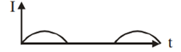
Physics Part Ii Chapter 14 Semiconductor Electronics: Materials, Devices And Simple Circuits
  • Sponsor Area

    NCERT Solution For Class 12 Physics Physics Part Ii

    Semiconductor Electronics: Materials, Devices And Simple Circuits Here is the CBSE Physics Chapter 14 for Class 12 students. Summary and detailed explanation of the lesson, including the definitions of difficult words. All of the exercises and questions and answers from the lesson's back end have been completed. NCERT Solutions for Class 12 Physics Semiconductor Electronics: Materials, Devices And Simple Circuits Chapter 14 NCERT Solutions for Class 12 Physics Semiconductor Electronics: Materials, Devices And Simple Circuits Chapter 14 The following is a summary in Hindi and English for the academic year 2021-2022. You can save these solutions to your computer or use the Class 12 Physics.

    Question 1
    CBSEENPH12039428

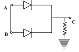
    A student wants to use two p-n junction diodes to convert alternating current into direct current. Draw the labelled circuit diagram she would use and explain how it works.

    Solution

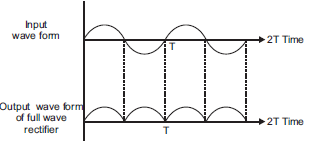
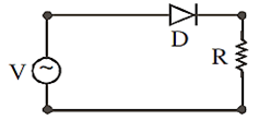
    The circuit of full wave rectifier is as shown below;

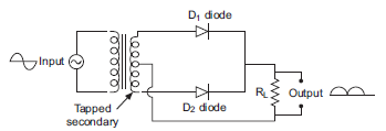
    Principle: The underlying working principle of full wave rectifier is that the p-n junction conducts when it is forward biased and does not condut when it is reverse biased.

    Question 2
    CBSEENPH12039429
    Question 4
    CBSEENPH12039586

    A p–n junction (D) shown in the figure can act as a rectifier. An alternating current source (V) is connected in the circuit.

    Solution

    C.

    Only +ve current passes though the diode. Given figure is half wave rectifier.

    Question 5
    CBSEENPH12039587
    Question 9
    CBSEENPH12039624
    Question 17
    CBSEENPH12039664

    Sponsor Area

    Question 18
    CBSEENPH12039665

    The circuit has two oppositely connect ideal diodes in parallel. What is the current following in the circuit?

    • 1.33 A

    • 1.71 A

    • 2.00 A

    • 2.31 A

    Solution

    C.

    2.00 A

    D1 is reverse biased therefore it will act like an open circuit.

    straight i equals space 12 over 6 space equals space 2.00 space straight A
    Question 20
    CBSEENPH12039681

    In a common base amplifier, the phase difference between the input signal voltage and output voltage is

    • π/4 

    • π

    • 0

    • π/2

    Solution

    C.

    0

    No phase difference between input and output signal.

    Question 21
    CBSEENPH12039721

    The thermistors are usually made of

    • metals with low temperature coefficient of resistivity

    • metals with high temperature coefficient of resistivity

    • metal oxides with high temperature coefficient of resistivity ‘

    • semiconducting materials having low temperature coefficient of resistivity.

    Solution

    C.

    metal oxides with high temperature coefficient of resistivity ‘

    These are devices whose resistance varies quite markedly with temperature mean having high-temperature coefficient of resistivity. [Their name are derived from thermal resistors]. Depending on their composition they can have either negative temperature coefficient or positive temperature coefficient or positive temperature coefficient or positive temperature coefficient characteristics. The negative temperature coefficient types consist of a mixture of oxides of iron, nickel and cobalt with small amounts of other substance. The positive temperature coefficient types are based on barium titanate.

    Question 22
    CBSEENPH12039740

    When npn transistor is used as amplifier

    • electrons move from base to collector

    • holes move from emitter to base

    • electrons move from collector to base

    • holes move from base to emitter.

    Solution

    A.

    electrons move from base to collector

    When npn transistor is used, majority charge carrier electrons n type emitter move from emitter to base and then base to collector.

    Question 23
    CBSEENPH12039741

    For a transistor amplifier in common emitter configuration having load impedance of 1 kΩ (hfe = 50 and hoe = 25) the current gain is

    • -5.2

    • -15.7

    • -24.8

    • -48.78

    Solution

    D.

    -48.78

    For a transistor amplifier in common emitter configuration, current again
    straight A subscript straight i space equals space minus space fraction numerator straight h subscript straight f subscript straight e end subscript over denominator 1 plus straight h subscript oe straight R subscript straight L end fraction
therefore space straight A subscript straight i space space equals space fraction numerator 50 over denominator 1 plus space 25 space straight x space 10 to the power of negative 6 end exponent space straight x space 1 space straight x space 10 cubed end fraction space equals space minus space 48.78
    where  hfe and hoe are hybrid parameters of a transistor

    Question 24
    CBSEENPH12039742

    A piece of copper and another of germanium are cooled from room temperature to 77 K, the resistance of

    • each of them increases

    • each of them decreases

    • copper decreases and germanium increases

    • copper increases and germanium decreases.

    Solution

    D.

    copper increases and germanium decreases.

    Copper is metallic conductor and germanium is semiconductor therefore as temperature decreases resistance of good conductor decreases while for semiconductor it increases.

    Question 25
    CBSEENPH12039743

    The manifestation of band structure in solids is due to

    • Heisenberg’s uncertainty principle

    • Pauli’s exclusion principle

    • Bohr’s correspondence principle

    • Boltzmann’s law

    Solution

    B.

    Pauli’s exclusion principle

    According to Pauli's exclusion principle, the electronic configuration of a number of subshells existing in a shell and number of electrons entering each subshell is found. Hence, on the basis of Pauli's exclusion principle, the manifestation of band structure in solids can be explained.

    Question 26
    CBSEENPH12039744

    When p-n junction diode is forward biased

    • the depletion region is reduced and barrier height is increased

    • the depletion region is widened and barrier height is reduced.

    • both the depletion region and barrier height reducedboth the depletion region and barrier height reduced

    • both the depletion region and barrier height increased.

    Solution

    C.

    both the depletion region and barrier height reducedboth the depletion region and barrier height reduced

    When p-end of the p-n junction is connected to positive terminal of battery and n-end to the negative terminal of a battery, then p-n junction is said to be forward bias. In forward bias, the more numbers of electrons go from n-region to p-region and more numbers of holes go from p-region to n-region. Therefore, major current due to both types of carriers takes place through the junction causing a reduction in height of depletion region and barrier potential.

    Question 28
    CBSEENPH12040114

    Which one of the following represents forward bias diode?

    Solution

    A.

    In forward bias, a p-type semiconductor is at higher potential w.r.t. n-type semiconductor.

    Question 29
    CBSEENPH12040115
    Question 31
    CBSEENPH12040145

    In the circuit shown in the figure, the input voltage Vi is 20 V, VBE = 0 and VCE = 0. The values of IB, IC and β are given by

    • IB = 40 μA, IC = 10 mA, β = 250

    • IB = 25 μA, IC = 5 mA, β = 200

    • IB = 40 μA, IC = 5 mA, β = 125

    • IB = 20 μA, IC = 5 mA, β = 250

    Solution

    C.

    IB = 40 μA, IC = 5 mA, β = 125

    VBE = 0,

    Vi  = 20 V

    VCE = 0

    Vb = 0 (earthed)

    Ic(20-0)4 x 103 = 5 x 103 = 5 mA

    Or

    Vi = 0 + IBRB

     20  = IB x 500 x 103 IB = 2500 x 103 = 40μAβ = ICIb = 25 x 10-340 x 10-6 =125

    Question 32
    CBSEENPH12040146

    In a p-n junction diode, change in temperature due to heating

    • Affects only reverse resistance

    • Affects only forward resistance

    • Affects the overall V - I characteristics of p-n junction

    • Does not affect resistance of p-n junction

    Solution

    C.

    Affects the overall V - I characteristics of p-n junction

    On heating, a number of electron-hole pairs increases, so overall resistance of diode will change.

    Hence, forward biasing and reversed biasing both are changed.

    Question 33
    CBSEENPH12040163

    The following circuit represents

    • OR gate

    • XOR gate

    • AND gate

    • NAND gate

    Solution

    B.

    XOR gate

    Output of upper AND gate = AB

    Output of lower AND gate = AB

    Thus, the output of OR gate = AB + AB

    This is boolean expression for XOR gate.

    Question 34
    CBSEENPH12047721

    The amplification factor of a triode valve is 15. If the grid voltage is changed by 0.3 V, the change in plate voltage in order to keep the current constant (in volt) is :

    • 0.02

    • 0.002

    • 4.5

    • 5.0

    Solution

    C.

    4.5

    μ = 15, ΔVg =0.3

     μ = VpVgVp =μ Vg               = 15×0.3               = 4.5 V

    Question 35
    CBSEENPH12047740

    Zener diode is used for

    • producing oscillations in an oscillator

    • amplification

    • stabilisation

    • rectification

    Solution

    C.

    stabilisation

    A zener diode is a silicon crystal diode having an unusual reverse current characteristic which is particularly suitable for voltage regulating purposes. Due to this characteristic, it is used as a voltage stabilizer in many applications in electronics.

    Question 36
    CBSEENPH12047745

    Carbon, silicon and germanium atoms have four valence electrons each. Their valence and conduction bands are separated by energy band gaps represented by EgC , EgSi and EgGe respectively. Which one of the following relationships is true in their case?

    • EgC > Egsi

    • EgC = EgSi

    • EgC < EgGe

    • EgC > EgSi

    Solution

    A.

    EgC > Egsi

    Crbon, silicon and germanium are semiconductors.

    Atomic number:- C - 6 ; Si - 14 and Ge -32 so all these semiconductors have 4 valence electron in their outermost shell.

    EgC = 5.2 eVEgSi = 1.21  eVEgGe = 0.75 eVThus,EgC > EgSi  &  EgC < EgGe

    Question 37
    CBSEENPH12047748

    Choose the only false statement from the following

    • Substances with energy gap ofthe order of 10 eV are insulators 

    • The conductivity of a semiconductor increases with  increases in temperature

    • In conductors the valence and conduction bands may overlap

    • The resistivity of a semiconductor increases with increase in temperature

    Solution

    D.

    The resistivity of a semiconductor increases with increase in temperature

    (a) In insulators energy gap is of the order of 5 to 10 eV and it is practically impossible to impart this much amount of energy to the electrons in valence band. So, as to jump to conduction band. So, choice (a) is correct.

    (b) In semiconductors with the rise in temperature more electrons from valence band jump to conduction band and this results is increase in conductivity. So, choice (b) is correct.

    (c) In conductors, the conduction band is either partially filled or the conduction band overlaps on the valence band. So, choice (c) is correct.

    (d) In semiconductor, resistivity decreases with increase in temperature. So, choice (d) is wrong.

    Question 38
    CBSEENPH12047750

    The total energy of an electron in the first excited state of hydrogen is about -3.4 eV. Its kinetic energy in this state is

    • -3.4 eV

    • -6.8 eV

    • 6.8 eV

    • 3.4 eV

    Solution

    D.

    3.4 eV

    The kinetic energy is equal to the negative of total energy.
    Kinetic energy of electron

    K = z e28 πεo rPotential energy of electron U = - 14πεo Ze2rTotal energy  E = K + U      = Z e28 πεor - Z e24 πεorE = -Ze28πεor

    ⇒ E  = - K

    ⇒  K = - E 

            = - ( - 3.4 )

    K = 3.4 eV 

    Question 39
    CBSEENPH12047812

    Which logic gate is represented by the following combination of logic gates?


    • OR

    • NOR

    • AND

    • NAND

    Solution

    C.

    AND

      Output of gate-1,  Y1 =A 

       Output of gate-2,  Y2 = B 

       Output of gate-3,

         Y = Y1 + Y2¯

             = A¯ B¯¯

             = A¯¯ B¯¯

         Y = AB

    which is the output of AND gate.

    Sponsor Area

    Question 40
    CBSEENPH12047821

    The principle of LASER action involves

    • amplification of particular frequency emitted by the system

    • population inversion

    • stimulated emission

    • All of the above

    Solution

    D.

    All of the above

    Laser action involves all the given phenomena
    (i) Amplification of particular frequency
    (ii) Population inversion
    (iii) Stimulated emission

    Question 41
    CBSEENPH12047822

    Which of the following is unipolar transistor?

    • p-n-p transistor

    • n-p-n transistor

    • Field effect transistor

    • Point contact transistor

    Solution

    C.

    Field effect transistor

    In Field effect Transistor  ( FET ) there is only one type of charge for conduction from drain to source i.e either electrons ( n-channel FET ) or holes (P-channel FET). 

    In NPN and PNP transistor both electron and holes take part in conduction. Hence they are bipolar Junction Transistor.

    Point contact Transistor is also Bipolar Junction Transistor.

    Question 42
    CBSEENPH12047839

    The truth table given below is for (A and B are the inputs, Y is the output)

    A B Y
    0 0 1
    0 1 1
    1 0 1
    1 1 0

    • NOR

    • AND

    • XOR

    • NAND

    Solution

    D.

    NAND

    The NAND gate is an AND gate followed by a NOT gate. If inputs A and B are both '1' the output Y is not '1'. The gate gets its name from this NOT AND behaviour.

    This is a logical symbol.

    The output Y is a combination of AND + NOT gate. Hence, the truth table is for NAND gate.

    Question 43
    CBSEENPH12047858

    Which logic gate is represented by the following combination of logic gates?


    • OR

    • NOR

    • AND

    • NAND

    Solution

    C.

    AND


                   Output of gate 1, Y1A¯                

                   Output of gate 2, Y2B¯

                    Outout of gate 3

                      Y = Y1 + Y2¯

                     Y = A¯ +B¯¯

                     Y  =A¯¯ × B¯¯

                     Y = AB

      Which the output of AND gate. 

    An AND gate has two or more inputs and one output. The output Y of AND gate is 1 only when input A and input B are both 1. 

    Question 44
    CBSEENPH12047864

    The reason of current flow in p-n junction in forward bias is

    • drifting of charge carriers

    • drifting of minority charge carriers

    • diffussion of charge carriers

    • All of the above

    Solution

    C.

    diffussion of charge carriers

    In forward biased condition, the width of the depletion region is very narrow. Hence, the free electrons and holes easily overcome the weak opposite electric field from the depletion region and cross the depletion region. Therefore, the electric current flows in the forward biased condition.

    Due to diffusion of charge carriers current flows throw in p-n junction.

    Question 45
    CBSEENPH12047897

    A change of 8.0 mA in the emitter current brings a change of 7. 9 mA in the collector current. The value of a will be

    • 0.96

    • 0.93

    • 0.90

    • 0.99

    Solution

    D.

    0.99

    We have

             IE = IB + IC

             ΔIE = ΔIB + ΔIC

    According to question,

              ΔIE = 8.0 mA

              ΔIC = 7.9 mA

        ∴    ΔI = 8.0 mA - 7.9 mA

               ΔI = 0.1 mA

      Now

              α = ICIE

    Where IC is the current flowing into the collector terminal

               IB is the current flowing into the base terminal

               IE is the current flowing into the emitter terminal

             α = ICIE 

                = 7.9 mA8.0 mA

              α  = 0.99        

    Question 46
    CBSEENPH12047931

    The truth table for the following logic circuit is

    • ABY000011101110

    • ABY001011101111

    • ABY001010101110

    • ABY001011100111

    Solution

    A.

    ABY000011101110

    The truth table for the given logic circuit is

    A B A¯ B¯ A¯ . B A . B¯ Y = A¯ B + A B¯
    0 0 1 1 0 0 0
    0 1 1 0 1 0 1
    1 0 0 1 0 1 1
    1 1 0 0 0 0 0

    Question 47
    CBSEENPH12047937

    The transfer ratio B of a transistor is 50. The input resistance of the transistor when used in the common emitter configuration is 2 kΩ. The peak value of the collector AC current for an AC input voltage of 0.02 V peak is

    • 200 μA

    • 0.01 mA

    • 0.25 mA

    • 500 μA

    Solution

    D.

    500 μA

    Given:-

    β = 50,

    R = 2 kΩ = 2 x 10³ Ω

    ΔVb = 0.02 V

    ic = ?

    Input current, 

                   ibVbRb

                       = 0.022000

                  ib = 10-5 A

    Also, current gain is the ratio of collector current to the base current.

                        β = icib

     ∴             ic = β ib

                        = 50× 10-5 A

                    ic = 500 × 10-6 A

                    ic = 500 μA 

    Question 48
    CBSEENPH12047956

    In the circuit shown in figure, when the input voltage of the base resistance is 10 V, Vb, is zero and Vce is also zero. Value of β is

    • 133

    • 154

    • 196

    • 105

    Solution

    A.

    133


    Given:- 

          Vi = 10 V

          Rb = 400 kΩ

               = 400 × 103 Ω

        Rc = 3 kΩ = 3 × 103 Ω

          Vbe = 0

          Vce = 0

          Vcc = 10 V

    As Vi - Vbe = RIb

        10 - 0 = ( 400 × 103 ) Ib

     ⇒        Ib103 × 103  

                    = 25 × 10-6 A

     ⇒        Ib = 25 μA

    and       Vcc - Vce = Ic Rc

     ⇒            Ic103 × 103

     ⇒                = 3.33 × 10-3

     ⇒         Ic = 3.33 mA

      β :- The ratio of collector current Ic to base current Ib

             β = IcIb

                = 3.33 × 10-325 × 10-6

               β = 133                       

    Question 49
    CBSEENPH12047967

    Assertion: An n-type semiconductor has a large number of electrons but still it is electrically neutral.

    Reason: An n-type semiconductor is obtained by doping an intrinsic semiconductor with a pentavalent impurity.

    • If both assertion and reason are true and reason is the correct explanation of assertion.

    • If both assertion and reason are true but reason is not the correct explanation of assertion.

    • If assertion is true but reason is false.

    • If both assertion and reason are false.

    Solution

    B.

    If both assertion and reason are true but reason is not the correct explanation of assertion.

    A n-type semiconductor is formed by doping pure germanium or silicon crystal with suitable impurity atoms of valency five. As the impurity atoms take the position of Ge atom in germanium crystal, its four electrons form covalent bonds by sharing electrons with the neighbouring four atoms of germanium whereas the fifth electron is left free. Since the atom, on the whole, is electrically neutral, the n-type semiconductor is also neutral.

    Question 50
    CBSEENPH12047984

    A transistor connected at common emitter mode contains load resistance of 5 kΩ and an input resistance of 1 kΩ. If the input peak voltage is 5 mV and the current gain is 50, find the voltage gain.

    • 250

    • 500

    • 125

    • 50

    Solution

    A.

    250

    Load resistance = 5 kΩ

    Input resistance = 1 kΩ

    β = 50

    Voltage gain Av = β × R0Ri

                            = 50 × 51

                   Av = 250

    Question 51
    CBSEENPH12047989

    The output for the given, circuit is


    •  A + B  · B¯

    • (A · B) · B

    • ( A + B )·B

    • ( A · B ) + B

    Solution

    A.

     A + B  · B¯

                  Y' = A + B

       and     Y = Y'. B¯

                 Y  = ( A + B ). B¯

    Question 52
    CBSEENPH12048007

    If the plate resistance oftriode valve is 13 x 106 Ω and amplification factor is 21. The mutual conductance will be

    • 1.6 × 10-6 mho

    • 1.6 × 106 mho

    • 2.6 × 10-5 mho

    • 2.6 × 105 mho

    Solution

    D.

    2.6 × 105 mho

    For triode value 

    Amplification factor 

             μ = rp × gm

    Here  rp = 13 × 106 Ω

             μ  = 21

            gm = ?

    ∴      gmμrp

                 = 2113 × 106

           gm = 1.6 × 10-6 mho

    Question 53
    CBSEENPH12048026

    Assertion:  A p-n junction with reverse bias can be used as a photo-diode to measure light intensity. 

    Reason:  In a reverse bias condition the current is small but it is more sensitive to change in intensity of incident light.

    • If both assertion and reason are true and reason is the correct explanation of assertion.

    • If both assertion and reason are true but reason is not the correct explanation of assertion.

    • If assertion is true but reason is false.

    • If both assertion and reason are false.

    Solution

    A.

    If both assertion and reason are true and reason is the correct explanation of assertion.

    The assertion and reason both are true.

    A photodiode is a p-n junction. When a photon of sufficient energy strikes the diode, it creates an electron-hole pair.

    By using reverse-bias condition, this reduces the response time because the additional reverse bias increases the width of the depletion layer, which decreases the junction's capacitance. The reverse bias also increases the dark current without much change in the photocurrent.

    Mock Test Series

    Sponsor Area

    Sponsor Area

    NCERT Book Store

    NCERT Sample Papers

    Entrance Exams Preparation